IoT Verification is Harder than it Looks

By Tom Anderson, Technical Marketing Consultant
As has been the case for at least 20 years, functional verification remains the bottleneck for semiconductor development. Many studies have shown that verification consumes 60-70% of a project’s time and resources. As more and more of the chip’s content comes from commercial intellectual property (IP) or reuse from previous generations, the ratio of effort tips even further toward verification.
The difficulties of verification are easy to understand if a system-on-chip (SoC) device is being developed. Each subsystem of the SoC is as large and complex as an entire chip in previous generations, with the added challenges of simultaneous operation and high-speed communication. The SoC contains one or more embedded processors, adding the hurdle of hardware/software co-verification to the project.
Designers of devices for applications in the Internet of Things (IoT) may think that they face less daunting verification challenges. They may look to bypass some aspects of verification, perhaps settling for lower coverage goals or an informal test plan that does not correlate intended functionality and coverage. In some cases, there may be little concern about long-term safety and reliability.
However, IoT teams do not “get a pass” when it comes to functional verification. While IoT devices are intended to be inexpensive and ubiquitous, easily tossed away and replaced when they fail or become outdated, many are in locations not easily accessible. This makes repair or replacement difficult. “Hidden” IoT devices may include factory automation equipment, security cameras, environmental sensors, and heating and cooling controllers.
Repair of such devices is feasible only if it can be accomplished with a software patch, but of course, not all hardware bugs have software workarounds. Also, for security reasons, some types of IoT devices may not be upgradable via the Internet. Complete replacement of IoT systems to fix chip bugs would be prohibitively expensive. Thus, just as for SoC designs, there are strong incentives to find and fix all bugs before the product is released.
Another key point is that many IoT chips are complex enough to quality as SoCs themselves. Architectures from Arm and Intel’s Atom family, both widely cited as good fits for IoT applications, now contain multiple processor cores and complex subsystems. Especially given the low-power requirements for battery-operated IoT devices, running slower processors in parallel may prove more efficient than a monolithic high-speed design.
Further, some high-end IoT chips are used in applications such as automotive electronics that have high requirements for safe operation. This means not only eliminating design errors but also planning for a proper response after a random event such as a strike by an alpha particle. In some cases, IoT manufacturers are required by their customers to meet strict functional safety standards such as IEC 61508 and ISO 26262.
Fortunately, formal verification technologies provide a wide range of solutions to address the challenges of IoT verification. Formal tools have the unique ability to uncover design bugs and prove mathematically that no such bugs remain to be found. This provides a measure of certainty impossible to obtain with simulation or emulation. This certainty extends beyond bugs to verification of hardware safety.
As a start, formal structural analysis automatically eliminates entire classes of design bugs. Unreachable code, unused signals, state-machine errors, synthesis-simulation mismatches, and other issues in the register-transfer level (RTL) design can be caught by the designer and fixed at the block level. It is often said that the cost of finding and fixing each bug grows 10 times from block to chip. Early bug discovery reduces project schedule and resources.
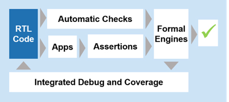
As blocks are integrated together, formal “apps” (applications) and verification IP (VIP) verify proper connectivity, X-propagation, protocol compliance, and other common elements of the chip-level verification plan (Figure 1). As with block-level checks, formal apps require minimal user input. They eliminate entire classes of bugs at the full-chip or full-system level automatically, with no need for the user to write properties or assertions.
Figure 1: Automatic checks and formal apps can verify many common types of design errors with little or no effort by the chip development team.
If the design and verification teams make the investment in assertions to express design intent, then an even wider range of design errors can be detected. Powerful formal engines analyze the design against the assertions, reporting any bugs found with extensive debug information, and reporting proofs if no bugs exist. Some types of blocks may be verified exclusively this way, while for others formal verification is a complement to simulation.
Even if the RTL code is free of design errors, bugs can also be introduced during the logic synthesis process due to errors in tools or methodology. Formal equivalence checking of the RTL design against the synthesized netlist has been part of the application-specific integrated circuit (ASIC) development flow for years. Running gate-level simulations on the netlist is slow and provides none of the certainly that only formal technology can provide.
Some IoT devices use field-programmable gate array (FPGA) technology, especially for applications with low volumes or tight time-to-market requirements. Equivalence checking is even more important for FPGAs than for ASICs. The FPGA synthesis/place-and-route flow often makes complex optimizations to the design, including re-timing by moving logic across cycle boundaries. Equivalence checking is the only reliable way to catch tool errors or inappropriate optimizations.
This formal-based flow satisfies the requirements of safety standards for a rigorous process to eliminate “systematic” (design) errors. These standards also mandate protection against random errors occurring in devices while in operation (Figure 2). Safety mechanisms must ensure that random errors are detected and either corrected or used to trigger an alarm. The chip development team must verify that the safety mechanisms work as intended.
Figure 2: Functional safety standards require a thorough, quantifiable verification process that addresses both design errors and faults from random events in the field.
Specialized formal apps analyze safety-critical designs to assess the effects of random faults, including determining which faults are “safe” because they do not affect normal functional operation of the chip. Formal apps also verify that the hardware safety mechanisms are working correctly and quantify the fault coverage provided by these mechanisms. Formal results can be intelligently combined with coverage from any fault simulator runs.
In general, merging the results of formal analysis with simulation is a key part of assessing overall verification progress and deciding when to move on to the next phase of the project. Planning how and where to use formal techniques occurs in the earliest stages of verification. Design requirements are mapped to features, each verified using the chosen engines, and the results from all engines are combined.
Verification of IoT semiconductor devices may appear easy at first glance, but this is rarely the case. Complexity of the designs and high-reliability requirements place a significant burden on the development team. Engineers must verify their chips thoroughly and guard against random events that can compromise operation. Proven formal tools and technologies to help are available today.
About the author
Tom Anderson is technical marketing consultant at OneSpin Solutions. His previous roles have included vice president of marketing at Breker Verification Systems, vice president of applications engineering at 0-In Design Automation, vice president of engineering at IP pioneer Virtual Chips, group director of product management at Cadence, and director of technical marketing at Synopsys. He holds a Master of Science degree in Computer Science and Electrical Engineering from M.I.T. and a Bachelor of Science degree in Computer Systems Engineering from the University of Massachusetts at Amherst.
