IP Integration Verification at DVClub Europe
By Sasa Stamenkovic, OneSpin Solutions
The online, free event will be held on 8 September 2020 and will explore solutions to the challenge of integrating in-house and third-party IPs into complex SoCs. Event Link Here --> www.testandverification.com/conferences/dvclub/europe/dvclub-europe-september-2020-ip-integration-into-complex-socs


Most people involved in pre-silicon verification of digital designs and electronic design automation (EDA) know the folks at Test and Verification Solutions (T&VS – now acquired by Tessolve to offer a full VLSI and test service). Among other things, they organize the Verification Futures (VF) conference in the UK and the DVClub Europe meetings. These are highly technical events, with plenty of interesting, cutting-edge technology presentations. Both VF and DVClub have been run as hybrid – physical at multiple locations and online - events for a long time, well before the COVID-19 situation. T&VS has done a great job making these events successful, benefitting the engineering community in the UK and worldwide. Kudos to Mike Bartley and his entire team!
The next DVClub Europe will be held on 8 September 2020, covering the topic of IP integration into complex SoCs. Modern, complex SoC development projects rely heavily on the availability of a vast library of third-party and in-house semiconductor intellectual properties (IPs). Even putting aside considerations about the availability of an adequate ecosystem, creating high-quality, configurable IPs from scratch is a time-consuming, difficult task, which can be justified only in specific circumstances. Four related, essential questions to consider are:
- Is there an existing IP that satisfies the project requirements?
- Would a new IP implement features that are critical to making the product commercially viable?
- Would a new IP be reused in multiple projects and product derivatives?
- If a suitable IP exists, how much does it cost to integrate it into the SoC?
The fourth question is not only about licensing and royalties. Integrating an IP into a complex SoC is not a simple plug-and-play task. Even a non-critical IP that is not integrated correctly or that is of substandard quality can compromise the integrity of the entire SoC.
IP Integration Challenges
Most IPs are integrated using their RTL model, before synthesis and other integrated circuit (IC) implementation steps. Ideally, IP users should have no reason to doubt that the RTL model is functionally correct. In practice, though, it is worth reviewing the IP verification evidence and environment at least, and check that the chosen IP configuration has been verified and used in other projects. The thoroughness of verification can vary dramatically from one IP to another, and, within an IP, from one configuration to another. The SoC developers are responsible for the correct integration of the IP in their system. A simple task like wiring can become challenging even for a single IP. There could be multiple instances and tens of thousands of input/output (I/O) ports to connect.
IPs integrated into safety-critical SoCs that have to comply with a functional safety standard, ISO 26262 for example, have to provide additional, safety-related documentation and evidence. The Accellera Functional Safety Working Group is, among other things, attempting to standardize data exchange and traceability of safety information from IPs to higher levels of the IC supply chain.
Finally, trust and security also need to be considered. Trust into the IP provider cannot be simply assumed. In security- and safety-critical applications, IPs and their providers should be vetted accordingly. While there are no standardized processes yet, technologies that automate this task are emerging. As for security, another Accellera initiative, the IP Security Assurance Working Group, aims to standardize the security-relevant information provided with IP to enable independent checking through commercial EDA tools and streamline the process of assessing the impact of IP-level security features on the SoC.
OneSpin, as a provider of certified IC integrity verification solutions, is a proud member of both the safety and security Accellera working groups.
Connectivity Checking
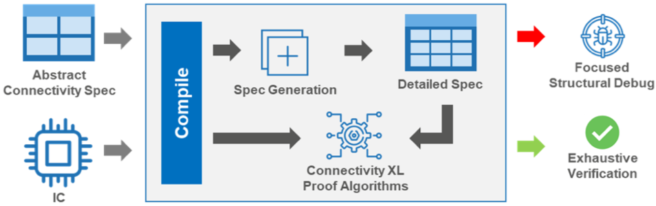
I have already mentioned that connectivity checking is a fundamental IP integration verification task. Global signals such as clock, reset, scan enable, and debug enable must be routed correctly across the chip. Bus interface signals may be wired through multiple hierarchy levels. The limited number of IC I/O pads available are exploited using layers of multiplexing logic, allowing many alternative connection configurations between pads and internal signals. Connection paths may go through register stages. Multiple power and clock domains pose additional connectivity requirements. Certain connectivity errors could only be visible under specific hardware configurations and input scenarios. The number of valid combinations is huge and hard to foresee. Relying on constrained-random testing or SoC-level use-case verification to hit as many corner-case connectivity scenarios as possible is neither an effective nor a rigorous approach. Formal, on the other hand, provides exhaustive verification. Moreover, debugging connectivity failures in formal is much easier compared to simulation, where the consequences of a wrong connection may become visible only after thousands of clock cycles.
However, modern ASIC and FPGA designs may have many hundreds of thousands of deep connections to verify. The computational challenge is enormous. Furthermore, creating the connectivity specification is a time-consuming, error-prone task. Most formal connectivity checking apps do not scale to extra-large chips.
At the upcoming DVClub meeting, OneSpin will drill into this topic with a presentation titled IP Integration Verification in Extra-large (XL) SoCs.
Xilinx’s Flow
Xilinx has addressed its connectivity checking challenges using a new flow based on the Connectivity XL app from OneSpin. They applied this flow to a multi-billion-gate, 7nm FPGA SoC after multiple state-of-the-art formal connectivity checking apps were tried unsuccessfully. The Xilinx design integrated more than 35 thousand modules with 60 million instances and included over 90 million flops and 80 thousand finite state machines (FSMs). The number of connections that needed to be specified, maintained across design iterations, and verified exceeded one million. Moreover, connections could have variable delays across design iterations and over two thousand signals in their path. With Connectivity XL, Xilinx was able to use an abstract connectivity specification and eliminate inconclusive proofs. The process identified several connectivity bugs that could be debugged quickly. Using the app’s reporting of connectivity paths, Xilinx implemented additional custom checks, for example to ensure that no signal in a path would violate certain high-level design rules. To learn more about Xilinx’s experience, download the paper “Scaling Formal Connectivity Checking to Multi-Billion-Gate SoCs with Specification Automation,” and don’t miss the next DVClub!
